All section Close
For Her Contribution To Materials Science, This IIT Kharagpur Alumni Won European Materials Research Society Award
20 March 2017 12:33 PM GMT
Editor : Koshika Mira Saxena Mira Saxena

Writer, social worker, book addict, love kids and cooking. Believes in spreading smiles.
The innovation and research ecosystem in India presents a significant and important opportunity for many people and organisations around the globe. Despite unenthusiastic science funding and government spending, Indian scientists have endeavoured admirably. India was ranked 13th globally according to a number of papers published in top journals. This was studied by a Nature Index report which presented a refreshing picture of Indian science showing a marked growth in high-quality scientific publication between 2012 and 2014 and revealed a particular strength in the broad discipline of chemistry.
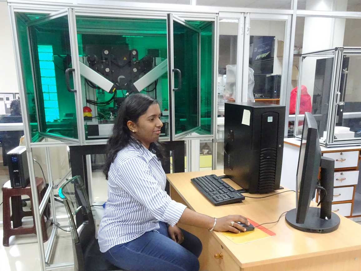
The Logical Indian interviewed Nandini Bhandaru, who herself is a researcher with a keen interest in nanotechnology. Nandini is a Chemical Engineer who has recently completed her PhD under the supervision of Professor Rabibrata Mukherjee at the Department of Chemical Engineering at Indian Institute of Technology (IIT), Kharagpur, West Bengal. She has been awarded the European Materials Research Society Award for her contribution to materials science and nanotechnology, mainly non-patterning of soft films and surfaces. She has also been conferred the prestigious Young Scientist Award from the Indian Science Congress Association in 2017.
The Logical Indian had a conversation with her about her journey and the research she has done.
What was the area of your research? What projects have you worked on?
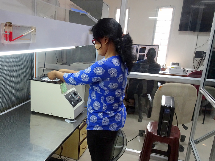
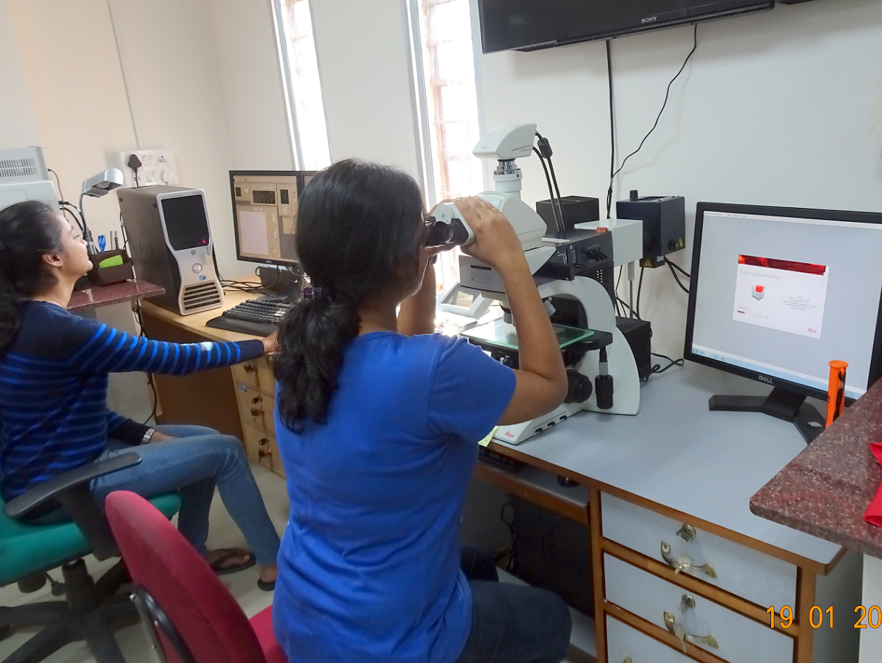
My area of doctoral research is nano-fabrication, which included soft-lithography, thin film dewetting, polymer blend films, and self-assembly. I have worked on several projects which, in simple terms, are related to organising things at the nanoscale. Under the mentoring of Professor Rabibrata Mukherjee, I, along with my colleagues at Instability and Soft Patterning Laboratory, have worked on developing methodologies for fabrication and manipulation of polymeric nanostructures by combining the essential concepts of top-down soft-lithography and bottom-up spontaneous instability in thin films.
The nanopatterns have been put to use in various fields of solar cells, microfluidics, and nanotechnology. Our team has also developed a new nanopatterning technique which has a unique ability to create nanoscale surfaces of any dimension without demanding any expensive instruments making the process cost friendly.
The method utilises elastic polymers and is so simple that it can be implemented by non-experts in a high school level laboratory. With the flexibility of creating any form of nanostructures over large areas, it becomes possible to create hydrophobic surfaces with controlled wettability and even superhydrophobic surfaces with self-cleaning properties. Such surfaces are similar to lotus leaves from which a water drop rolls off automatically and takes along with it any accumulated dust.
We have also developed a technique for creating ordered nanodomains in polymer blend films (a mixture of two or more polymers) using patterned templates. Such multi-component films find wide application in various areas such as plastic solar cells and biological scaffolds. For example, controlling the nano-morphology of the donor–acceptor blends in organic solar cells can lead to an enormous increase in the electron conversion efficiency.
Furthermore, the presence of nanostructures provides anti-reflective and self-cleaning properties to the surface of the solar cells. This significantly enhances the overall efficiency and life of a solar cell. In collaboration with a group in School of Medical Science and Technology at IIT-KIharagpur, we looked into the development of a polymer blend based nanostructured therapeutic patches having dual behaviour on cells isolated from different conditions (normal, pre-cancer, and cancerous). The presence of the patterns confines the adhesion and propagation of cancer-associated cells, thereby limiting their growth.

What is nanofabrication?
“Nano” represents 10^-9 metres. To give an idea of how small it is, we are essentially talking about things roughly 1/1000th times the width of human hair.
Things at this scale find wide application in various areas such as in electronic devices, data storage media, optoelectronic devices, cancer therapeutics and so on. For most of these applications, rapid prototyping of nanostructures over large areas (~cm^2) is necessary. But the conventional machine-based fabrication approaches fail because our hands do not work at the nanoscale; even the most high-end equipment have limitations. Though some techniques like photolithography or electron-beam writing are capable of generating structures with lateral feature resolution down to 10 nanometres, these methods require expensive instrumentation, making them unsuitable for rapid, large-area or bulk fabrication. Also, the expenses involved in such fabrication methods is significant. For example, a single nanopatterned mask may cost around $500-$2000 based on complexity of design.
In fact, the forces at nanoscale are completely different from our macroscopic world as gravity – the most important force – has no role in the nano world. On the other hand, making things smaller actually adds new properties to a material; an insulating material may start conducting at nanoscale, a hydrophilic surface can become hydrophobic, gold which has yellow lustre becomes reddish or dirty brown when in the form of nanoparticles. Hence incorporating nanostructures will have direct impact on a lot of application in our day-to-day life.
What process did you use?
The techniques we have developed are based on fundamental aspects related to confinement-induced instability, morphological evolution, and pattern formation. The multi-component thin films comprising of two immiscible (of liquids, not forming a homogenous mixture when mixed) polymers either in the form of a bilayer (stacked layers) or blend (homogeneous mixture). This fascinating branch of science that has overlap with nanotechnology, microfluidics and surface engineering has received significant attention in the last couple of decades. Such instability leads to self-assembled meso scale structures. However, the structures are inherently isotropic and thus have limited practical utility.
The key objective of my research is to order and align these structures by laterally confining the morphological evolution during the instability, which has been achieved using topographically structured templates. This leads to the possible creation of a myriad of extremely novel polymeric nanostructures, which cannot be achieved by any existing technique or machinery.

How would it be helpful for people? What are its advantages?
Our principal aim is to devise techniques with which nanostructures and ordered nanopatterns can be created on any material in few simple steps, without the need of extensive instrumentation. By doing so, the fabrication cost typically involved in such fabrication can be reduced probably by 100 times. Thus the potential of nanotechnology can be fully leveraged. I have already mentioned about one major application where the chances of recurrence of oral cancer after a surgery are found to be minimised or removed by using a novel handmade path comprising of certain form of nano structures. I will give one more example: touchscreens have become the major mode of interaction with any device, including smartwatches, smartphones, tablets, displays, control panels etc. These surfaces are continuously in contact with human body and hence get covered with body grease and fingerprint contaminant, which has become a major concern as this reduces visibility as well as device efficiency. To avoid this, the touch screens need to be covered with easy-to-clean coatings which could cause the print contaminants not to spread or deposit over large areas, and also provide an easy cleaning mechanism such as a gentle dry wipe. This is a concept we are presently working on based on our technique of developing superhydrophobic surfaces.
Where are you planning to take this further?
Most of the techniques and some of the products developed by the group have been patented. We are now working towards upscaling the techniques for suitable applications and also planning to have some industrial collaboration.
Do you have any message for our readers?
Research and development are two of the major areas which our country must focus on for overall growth. I personally feel that choosing to continue my higher studies and pursuing research instead of opting for a lucrative job was one of my best decisions. Also, working under the extraordinary guidance of Prof. Mukherjee, I realised how fulfilling research could be – one can be creative, explore the world of science and at the same time immensely contribute to the society. I would also like to encourage more young women to pursue higher education and research. Multiple universities, institutes, and companies have realised that a strong R&D is necessary for becoming world leaders in any field and are promoting and funding research activities.
Must Reads
We are an independent and public-spirited digital media platform for Indian millennials. We report news and issues that matter as well as give you the opportunity to take action.